
Op Amp PCB Layout: A Comprehensive Guide for Designers
When it comes to designing a PCB with operational amplifiers (op-amps), attention to detail is paramount. The layout of an op-amp circuit can significantly impact its performance, stability, and overall functionality. In this article, we will delve into the intricacies of op-amp PCB layout, providing you with a multi-dimensional introduction to ensure your designs are optimized for success.
Understanding Op-Amp PCB Layout Basics

Before diving into the specifics of op-amp PCB layout, it’s essential to have a solid understanding of the basics. An op-amp PCB layout involves careful placement of components, routing of traces, and consideration of power and ground planes. Let’s explore these aspects in more detail.
Component Placement
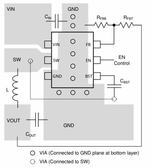
Proper component placement is crucial for minimizing noise and ensuring optimal performance. Place the op-amp close to the power supply and ground pins to reduce the length of the power and ground traces. Additionally, position the op-amp near the input and output signals to minimize the length of these traces as well.
Trace Routing
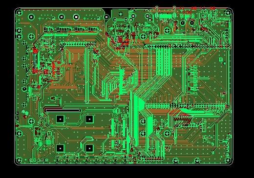
Trace routing plays a vital role in op-amp PCB layout. Keep the traces as short as possible to reduce noise and improve signal integrity. Avoid routing traces over high-noise areas, such as digital circuits, and use wide traces for high-current paths. Utilize proper via placement to connect layers and maintain a clean layout.
Power and Ground Planes
Power and ground planes are essential for providing a stable reference for the op-amp circuit. Place the power and ground planes close to the op-amp and ensure they are well-connected to the power supply and ground pins. This helps to reduce noise and improve the circuit’s performance.
Op-Amp PCB Layout Best Practices
Now that we have covered the basics, let’s explore some best practices for op-amp PCB layout. These guidelines will help you create a well-designed and high-performing circuit.
Minimize Loop Area
Minimizing loop area is crucial for reducing noise and improving the circuit’s performance. Keep the power and ground traces close to each other and ensure they are well-connected to the power supply and ground pins. This helps to minimize the loop area and reduce noise.
Use Proper Decoupling Capacitors
Decoupling capacitors are essential for providing a stable power supply to the op-amp. Place decoupling capacitors close to the power supply pins and ensure they are connected to the ground plane. This helps to reduce noise and improve the circuit’s performance.
Avoid High-Speed Traces
Avoid routing high-speed traces near sensitive circuits, such as the op-amp input and output. High-speed traces can introduce noise and degrade the circuit’s performance. If high-speed traces are necessary, use proper termination techniques to minimize the impact on the circuit.
Op-Amp PCB Layout Tools and Techniques
Several tools and techniques can help you create an effective op-amp PCB layout. Let’s explore some of these options.
PCB Design Software
PCB design software, such as Altium Designer, Eagle, and KiCad, is essential for creating an op-amp PCB layout. These tools provide features for component placement, trace routing, and power and ground plane management. Familiarize yourself with the software’s capabilities to create a well-designed PCB.
Simulation Tools
Simulation tools, such as LTspice and Multisim, can help you verify the performance of your op-amp circuit before manufacturing. Use these tools to test different design configurations and optimize your circuit for the best performance.
Layout Guidelines
Several online resources provide layout guidelines for op-amp circuits. These guidelines can help you make informed decisions about component placement, trace routing, and power and ground plane management.
Op-Amp PCB Layout Case Studies
Let’s take a look at some real-world examples of op-amp PCB layouts to gain a better understanding of the design process.
Case Study 1: Audio Amplifier
In this case study, we will examine the PCB layout of an audio amplifier using an op-amp. The design focuses on minimizing noise and ensuring optimal audio quality. The component placement, trace routing, and power and ground plane management are carefully optimized for the best performance.